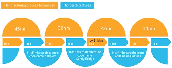
Intel is set to roll out its latest generation of processors this spring despite a minor setback affecting ultra low-voltage models – the ones destined for super slim notebooks. By normal standards, the launch should mark a new "tick" in the company's product roadmap, but Intel is going beyond just shrinking the current 32nm Sandy Bridge processor by introducing some fundamental advancements along with its new 22nm process.
For those unfamiliar, Intel follows a "tick tock" model for its processor upgrade cycle. With every "tick" the company moves to a smaller manufacturing process, from 32nm to 22nm in this case, dramatically increasing transistor density while enhancing performance and energy efficiency of the current microarchitecture. Then, with an alternating "tock" cycle Intel introduces a new processor microarchitecture.

Ivy Bridge includes manufacturing and subsystem improvements. It is a shrink of Sandy Bridge and is also the first to us Intel's Tri-Gate transistors, which use a nonplanar architecture to cram more transistors into less space, therefore consuming less power or delivering more performance within the same power envelope.
There's been quite a bit of information on Ivy Bridge going around ever since Intel detailed the architecture late last year. We'll recap some of the major changes and practical implications, while also bringing you up to speed on the latest developments, including expected launch lineup and specs.
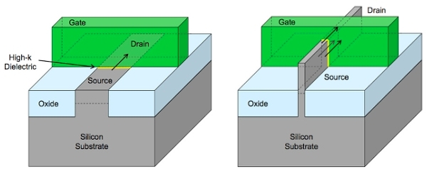
Unlike conventional planar transistors that lay flat, Ivy Bridge's Tri-Gate transistors use a three-dimensional fin that stands vertically from the silicon substrate. This presents several benefits. For starters, Intel can cram more transistors into less space, which will be incredibly valuable as fabrication tech shrinks to 22nm and beyond.
In addition, the new design allows for essentially three times the surface area for electrons to travel when the transistor is in the 'on' state, which paves the way for increased performance.

Transistors carry an electrical signal while gates control that flow by turning the current on and off. Whereas in a typical transistor only the small layer between the channel and the gate becomes active when the transistor is switched on, Intel's Tri-Gate transistor creates a three-sided silicon fin that the gate wraps around, increasing the surface area where electrical current actually flows. The video below does a better job explaining this.
This design also maximizes transistor switching performance between on and off states and decreases power-wasting leakage.
Intel summarizes the practical implications by saying the 22nm 3D Tri-Gate transistors provide up to a 37% performance increase at low operating voltages versus Intel's 32nm planar transistors – a big deal for Atom and ULV chips – or close to 20% at 1V for higher end desktop and mobile parts.

Intel has also mentioned the possibility to have multiple fins standing vertically from the silicon substrate and connected together, as shown to the right, to increase total drive strength of the transistor for higher performance. They haven't discussed this in detail but we assume Intel could use it to more finely tune its 22nm process in higher end products, or use it as a fail-safe method to improve yields of individual dies.
The new 22nm Tri-Gate wafers shouldn't be much more expensive to produce, either. Compared to a hypothetical Intel 22nm planar process, the 3D Tri-Gate process should only add another 2-3% to the total cost, according to Intel's own estimates.
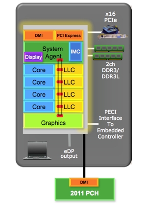
Besides the new transistor design there are no major changes in the Ivy Bridge architecture compared to Sandy Bridge. It continues the 2-chip platform partition (CPU + PCH) and is backwards compatible with existing LGA-1155 motherboards, although there will be new chipsets to enable new features.

All these components are bound by a ring-bus that transports data between them. The system agent has interfaces for the dual-channel DDR3 integrated memory controller, the PCI-Express controller (supporting 16 PCIe 3.0 lanes), the DMI chipset bus, a display controller, and FDI link to the PCH.
Graphics
But there are also a few tweaks here and there. First and foremost the graphics core has been completely redesigned and now supports OpenCL 1.1, DirectX 11 and OpenGL 3.1. This will finally bring the Intel integrated GPU to feature parity with AMD's. Intel also added a graphics-specific L3 cache, three display outputs (up from two in Sandy Bridge), better anisotropic filtering, more shaders or execution units (either 8 or 16 EUs in Ivy Bridge depending on the GPU versus 6 or 12 in Sandy Bridge), and a few other enhancements.
Ivy Bridge also greatly improves Intel Quick Sync Video, the chip giant's transcoding technology. All told, the end result is up to a 60% increase in GPU performance over Sandy Bridge's integrated GPU.
Hyper-Threading and CPU instruction set changes On the CPU side there are some changes in the way resource allocation for HyperThreading queue takes place. Ivy Bridge will dynamically allocate resources to threads so that if there is only a single thread active, all resources will be dedicated to that thread rather than some going unused as with SB's static allocation.
There's a new random number generation process that improves security, a power management feature that offers more flexibility in setting a system's thermal envelope (more on this next), and memory and string performance enhancements. Ivy Bridge also reportedly allows for more dynamic overclocking.
On the next two pages: Ivy Bridge's power optimizations & CPU and chipset confirmed launch line-ups.
